
ASML is one of the world’s leading manufacturers of chip-making equipment.
Our vision is to enable affordable microelectronics that improve the quality of life. To achieve this, our mission is to invent, develop, manufacture and service advanced technology for high-tech lithography, metrology and software solutions for the semiconductor industry.
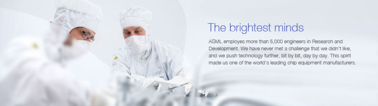
ASML's guiding principle is continuing Moore's Law towards ever smaller, cheaper, more powerful and energy-efficient semiconductors. This results in increasingly powerful and capable electronics that enable the world to progress within a multitude of fields, including healthcare, technology, communications, energy, mobility, and entertainment.
Working at ASML
We provide the world’s top chipmakers everything they need to create better performing, cheaper semiconductor chips. Simply put: we are an industry leader supporting industry leaders.
As such, you’ll be encouraged to bring your best ideas and act on them. You’ll have the freedom, trust, and support in your field to experiment and solve complex challenges. Things are rarely dull when you’re constantly breaking new ground.
But despite our fast-paced environment at the forefront of tech, we take your work-life balance and wellbeing seriously. A business is only as good as its employees.
So join us, and you’ll be a part of a global collaboration. One that promotes creativity, the inclusion of highly diverse teams, and an exciting and dynamic work environment. Join us, and you’ll be a part of progress.
Introduction
Working on the forefront of semiconductor manufacturing by designing integral application solutions around the world’s most advanced lithography tools.
Job Mission
One of the main key performance indicators (KPI) of lithography is overlay accuracy. The main competency of the On Product Performance Alignment group is the development of wafer fab applications that optimize the alignment between layers consisting of printed features on actual product wafers of our customers in order to improve overlay performance and thus contributing to customer’s yield and profitability.As a design engineer alignment you will design and support the implementation of alignment solutions that improve the overlay performance on actual product wafers. Your scope exceeds the overlay performance of ASML’s lithographic equipment, and includes effects on the on-product alignment performance caused by other processing equipment, masks, metrology, and the choices that are made by the customer on how to do process setup and control.You are responsible for creating and refining ASML’s application products that will improve the on-product performance of our customers. You will do this in close collaboration with the customer, and connected to the introduction of a new technology node in production of the customer. Your proposals for application product improvement can cover a wide variety of solutions concerning process fingerprint root cause analysis, choices in process control strategies, metrology mark choice and design and process optimization. The findings will also be used for improvement in the scanner modules.You are expected to represent ASML as an expert in the field and to get recognition for this by the customers. Since you will be working intimately with customers and sensitive customer data, a high level of integrity is required for securing confidentiality, while at the same time being able to translate these into ASML product improvements or new product developments.
Job Description
The job consists of following activities:
Education
MSc. Or BSc. degree in Physics, Mathematics or Engineering (Mechanical, Optical, Electrical, Chemical),
Experience
We are looking for people with a solid background in statistics, data analysis, optics, semiconductor process technology and semiconductor device physics. We are open for both entry as experienced candidates. So we have a wide range of 0-10 years of experience in an industrial research, development, or process control organization and preferably experience with overlay and/or wafer alignment within the semiconductor industry.
Personal skills
Travelling a few times per year to customers worldwide can be part of the job. An assessment is part of the selection process.
| Education Backgrounds: |
Mathematics Mechanical Engineering Physics |
| Specialties: |
Experimental Physics Optics Process Management Semiconductor Physics |
| Education Level: |
Undergraduate (Bachelors) Postgraduate (Masters) |
| Experience: |
0 - 2 years 5 - 10 Years |
| Languages spoken: |
English |
| Job Location: | Veldhoven, Netherlands |
| Keywords: | tatistics, data analysis, optics, semiconductor process technology, semiconductor device physics |

Type: Job
Deadline: 25th July 2026
Job reference (ID): 15270

Loading...