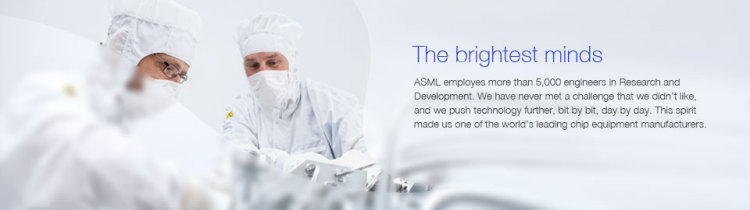
ASML is one of the world’s leading manufacturers of chip-making equipment.
Our vision is to enable affordable microelectronics that improve the quality of life.
To achieve this, our mission is to invent, develop, manufacture and service advanced technology for high-tech lithography, metrology and software solutions for the semiconductor industry.
ASML's guiding principle is continuing Moore's Law towards ever smaller, cheaper, more powerful and energy-efficient semiconductors. This results in increasingly powerful and capable electronics that enable the world to progress within a multitude of fields, including healthcare, technology, communications, energy, mobility, and entertainment.
Physics Design Engineer- Leveling and Wafer Alignment Job Description
Physics Design Engineer- Leveling and Wafer Alignment
Introduction
Are you experienced in defining functional specifications? Are you eager to take ownership of a problem and create a vision of how to solve it – a vision that also inspires others? Then the ASML Performance & Integration – Sensors department is your ideal environment for personal development and professional growth.
Job Mission
To contribute to the development of products by designing, creating, integrating and testing solutions to improve the Leveling and Wafer Alignment functionality, within the restrictions imposed by system specifications, costs and planning considerations.
Job Description
Responsibilities of a Designer in the Leveling or Wafer Alignment group:
- Participate in the definition of system level specification of the Leveling and Wafer Alignment function, like functionality, performance, cycle time and reliability.
- Perform feasibility studies into required improvements, by means of experiments, simulation and analysis of existing (customer) data.
- Design the functional specifications and required algorithms.
- Support the realization by giving input supporting specialist software designers in the project team.
- Integrate and test the function against the specification.
- Troubleshoot on issues within our factory or at customer sites
- Support sustaining activities.
Physics Design Engineer- Leveling and Wafer Alignment Job Requirements
Education
Master’s or PhD (Preferred) in Physics or Applied Mathematics.
Experience
Experience with functional specification and integration (data analysis - preferably with Matlab, modelling, defining functional specifications) is a prerequisite. You are experienced with design of algorithms and functional models.
Personal skills
- Team worker and excellent communicator
- Strong technical background and drive towards solutions.
- Solution minded and able to see and develop the bigger picture.
- Decisive and self-initiating
- Result focused and a “can do” spirit
- Ability to influence withoutpower.
Context of the positionWithin ASML, the sector Development & Engineering (D&E) is responsible for the specification and the design of the ASML products. The department Performance & Integration – Sensors is responsible for development, delivery, integration and qualification of functional modules & machine/customer applications on spec, within time and budget in the areas of overlay and focus.
Other informationASML creates the conditions that enable you to realize your full potential. We provide state-of-the-art facilities, opportunities to develop your talents, international career opportunities, a stimulating and inspiring environment, and most of all, the commitment of a company that recognizes and rewards outstanding performance.
Our selection process includes an online Talent Exploration that gathers information about your key drivers, your personal values, motivators and career ambitions. The Talent Exploration enables both you and us to explore if there is a mutual match - not only for today, but also for your future career at ASML.
Please add your complete & recent CV and cover letter for this position to your application.
We can't process your application without the above mentioned documents.
You can apply for this job using below button: “Apply for this job”.
Applications sent by email can’t be processed.
Physics Design Engineer- Leveling and Wafer Alignment Application Information
Please apply with your CV and cover letter by the 'apply' button below
Remember - you found this opportunity on Qreer.com
Physics Design Engineer- Leveling and Wafer Alignment Summary
Education Backgrounds: |
Mechanical Engineering Micro / Nano Technology Physics |
Specialties: |
Experimental Physics Laser/Photonics Optics Research (R&D) Semiconductor Physics
|
Education Level: |
Undergraduate (Bachelors) Postgraduate (Masters) Doctorate (PH.D)
|
Experience: |
0 - 2 years 2 - 5 years 5 - 10 Years
|
Languages spoken: |
English |
Job Location: |
Veldhoven, Netherlands |
Apply